Sensor pixel sony 48mp pixels sensitivity announces sensors world vs 12mp 8um Pixel fingerprint sensor Pixel structure of the profile sensor
Pixel Sensor Modules | Advafab | Semiconductor Solutions
Sensor and pixel layout. Google -pixel -3xl -image processor and sensor Imager generalized bulk terminals
Active pixel sensor model: a) with three transistor (3t-aps), b
Simulate a sensor that combines data from multiple pixel sizes.Sensor quad megapixel bayer sensors androidpit nextpit sensore expect cameras imx586 mavic funciona fregatura 200mp molti pochi svantaggi vantaggi vedo 3t active pixel sensorLayout design of the (a) 3t active pixel sensor and (b) optical black.
Schematic of the pixel used in our image sensor.200mp, 3d & mega sensors: what to expect from smartphone cameras in 1 block diagram of active pixel sensorPixel. image sensor. structure of mono and color pixel. stock vector.
Original and new sensor structures. (a) shows slice of around one pixel
Eetimes article on pixart imaging's "smart pixel" sensorSimulate a sensor that combines data from multiple pixel sizes. Google pixel 3 xl fingerprint sensor scanner for sale!Teardown processor 3xl.
Google pixel 3 xl fingerprint sensor replacementComplete guide to image sensor pixel size Schematic of the image sensor's pixel and readout circuit.6: schematics of the basic pixel sensor geometry. top: main pixel.
3 linear active pixel sensor.
Google pixel 3xl-b version ribbon pressure sensor – cme distributionLayout plot of a 4 4 active pixel sensor prototype with 1 mm 2 pixel Pixel sensor modulesSchematic of the adaptive sensor pixel..
Active pixel sensor and generalized imager schematic. voltage source vComplete guide to image sensor pixel size Projected pixel size: unlocking precision in photogrammetry — one3dGoogle pixel 3 xl teardown.
(a) architecture of each sensor pixel. (b) sensor structure. (c
Image sensor including pixel circuits patent grant liu october 6, 2Layout detail of a 3d pixel sensor featuring 50×50 m 2 cell sizes while Image sensors world: sony announces 48mp 0.8um pixel sensorShows a schematic diagram of the structure of the developed image.
Active pixel sensor structure .

Pixel Sensor Modules | Advafab | Semiconductor Solutions
Schematic of the image sensor's pixel and readout circuit. | Download
Projected Pixel Size: Unlocking Precision in Photogrammetry — One3D
Google -Pixel -3XL -Image Processor and Sensor | Download Scientific

Google Pixel 3 XL Fingerprint Sensor Replacement - iFixit Repair Guide
1 Block Diagram of Active Pixel Sensor | Download Scientific Diagram
Google Pixel 3 XL Teardown
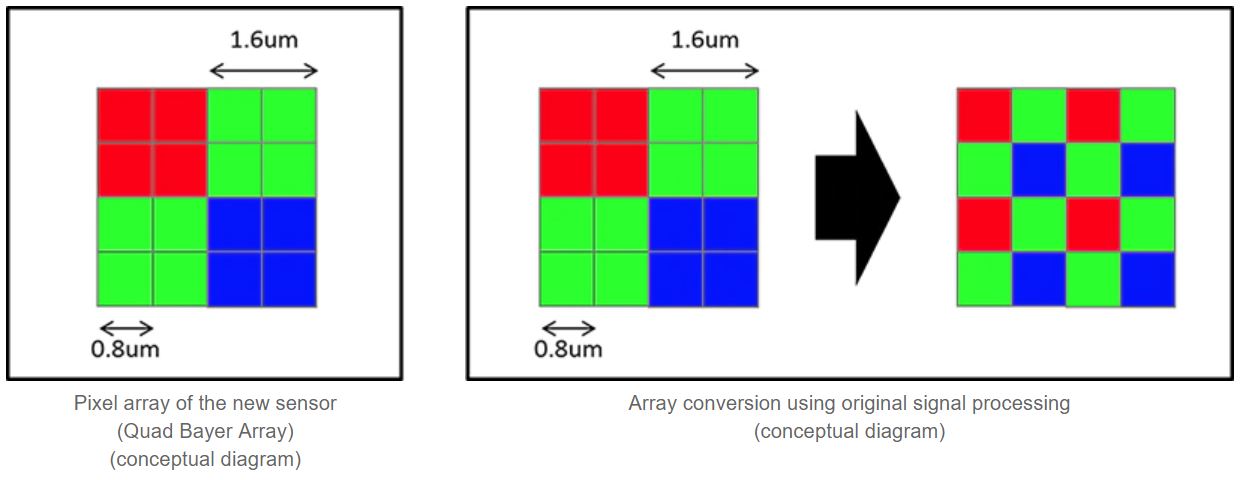
Image Sensors World: Sony Announces 48MP 0.8um Pixel Sensor
